
Advanced SWIR Camera Systems Enhance Semiconductor Quality Control
The Critical Need for Subsurface Defect Detection
Semiconductor manufacturing demands flawless quality control. Both surface and internal defects can compromise chip performance. Traditional vision systems often miss these hidden flaws. However, advanced inspection technologies now address this challenge effectively.
SWIR Technology: Seeing Through Silicon
Short-wave infrared cameras revolutionize semiconductor inspection. Silicon becomes transparent at specific SWIR wavelengths. This transparency enables visualization of internal structures. Consequently, manufacturers can detect subsurface defects invisible to standard cameras.
Semiconductor Market Growth and Quality Demands
Global semiconductor sales are projected to reach $728 billion (World Semiconductor Trade Statistics). This massive market expansion increases quality control importance. Every defective chip creates significant financial impact. Therefore, industrial automation systems must ensure maximum yield.
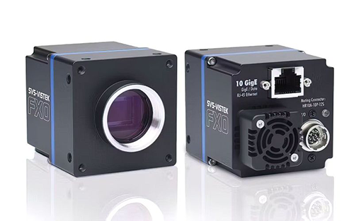
SVS-Vistek SWIR Camera Technical Specifications
SVS-Vistek SenSWIR FXO cameras offer exceptional capabilities:
5.2 megapixel resolution for detailed imaging
400-1700 nm spectral range coverage
Simultaneous SWIR and visible light capture
10GigE Vision and CoaXPress interfaces
Thermoelectric cooling option available
Integration Advantages for Factory Automation
These cameras simplify implementation in existing systems. GenICam 3.0 ensures standardized software integration. Moreover, the integrated strobe controller supports complex illumination scenarios. This compatibility makes them ideal for industrial automation environments.
Application Case: Semiconductor Wafer Inspection
A major semiconductor manufacturer implemented SVS-Vistek SWIR cameras. Their production line achieved 30% higher defect detection rates. Additionally, they reduced false rejections by 15%. This improvement significantly boosted their overall equipment effectiveness.
Future Trends in Industrial Vision Systems
The integration of AI with SWIR imaging represents the next frontier. Machine learning algorithms can analyze subtle defect patterns. Furthermore, factory automation increasingly demands real-time processing capabilities. These advancements will continue transforming quality control processes.
Expert Commentary from World of PLC
As industrial automation specialists, we recognize SWIR technology’s transformative potential. These cameras address critical challenges in semiconductor manufacturing. For comprehensive industrial automation solutions, explore our product portfolio at World of PLC. Our expertise ensures optimal system integration and performance.
Frequently Asked Questions
Why is SWIR imaging better than visible light for semiconductor inspection?
SWIR wavelengths penetrate silicon, revealing internal defects that visible light cannot detect.
What integration challenges exist when implementing SWIR cameras?
Modern SWIR cameras feature standard interfaces like GenICam, making integration straightforward in existing automation systems.
How does thermoelectric cooling improve image quality?
Active cooling reduces sensor noise, resulting in cleaner images and more accurate defect detection.
This article provides expert analysis on semiconductor inspection technologies. For specific implementation guidance, consult with qualified industrial automation engineers.


